
 来源:鼎纪电子PCB 发布日期
2017-03-23 浏览:
来源:鼎纪电子PCB 发布日期
2017-03-23 浏览:
AlTIum designer 信号完整性分析
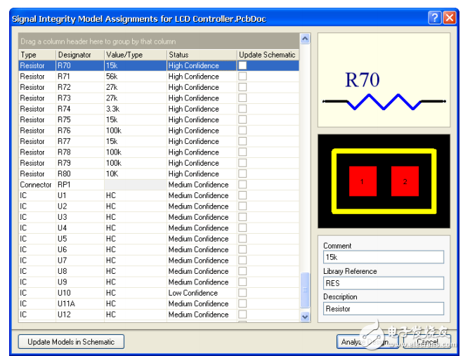
This tutorial looks at performing Signal Integrity (SI) analyses. It covers setTIng up design parameters like design rules and Signal Integrity models, starTIng up Signal Integrity from the SchemaTIc and PCB Editors, configuring the tests to be used in the net screening analysis, running further analysis on selected nets, terminating the signal line, setting preferences and working with the resulting waveforms. With Altium Designer, you can analyze the Signal Integrity performance of a PCB from either the Schematic or the PCB Editors, evaluate net screening results against predefined tests, perform reflection and crosstalk analysis on selected nets, and display and manipulate the waveforms in the Waveform Analysis window.
【本文标签】: 多层 pcb 多层PCB面板 公司设备 沉金板
【责任编辑】:鼎纪电子PCB 版权所有:http://www.dj-pcb.com/转载请注明出处
 扫一扫更精彩!